


01
Precision Machining Services for Electronics and Semiconductor Manufacturing
2025-08-11
Lorem Ipsum is simply dummy text of the printing and typesetting industry.
Lorm Ipsum has been the industry's standard
dummy text took a galley of type and scrambed it to make a type specimen
book. Lorem Ipsum is simply dummy text of the
printing and typesetting Lorem Ipsum is simply dummy text of the printing
and typesetting industry.Lorem Ipsum is simply
dummy text of the printing and typesetting industry.
Providing high-precision core components for the electronics and semiconductor industries
Why choose Kansd's precision machining services for electronics and semiconductors?
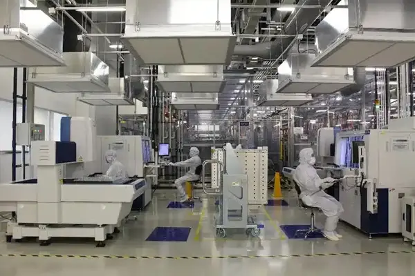
Shenzhen Kansd Technology Co., Ltd. (certified to ISO 9001:2015 & ISO 14001) is deeply rooted in the electronics and semiconductor manufacturing field. It is committed to processing semiconductor and electronic components with nanometer-level accuracy (±0.0005mm). Its business scope covers areas such as chip manufacturing equipment, semiconductor packaging, and core components of electronic products. It has delivered over 5 million high-precision parts, effectively helping customers improve product performance and production efficiency.
Core Advantages
1. Compatible Material System
Full Material Coverage: It covers a variety of materials such as silicon wafers, silicon carbide, gallium nitride, aluminum alloy 6061-T6, and copper alloy C11000, meeting the requirements of different electronics and semiconductor devices in terms of performance, heat dissipation, and dimensional stability.
Structural Compatibility: It supports the processing of complex structural parts such as chip carriers (thickness tolerance ±0.01mm) and semiconductor equipment vacuum chambers (surface roughness Ra0.2μm).
2. Mass Production-Level Precision Control
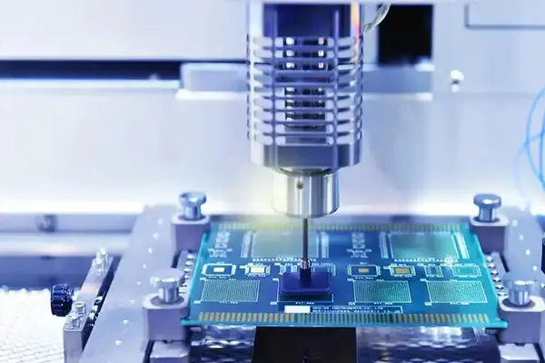
Strict Tolerance Standards: The machining accuracy of CNC milling is ±0.002mm, and the lithography alignment accuracy is ±0.0005mm.
Flatness Calibration: For semiconductor wafer processing, the surface flatness of the wafer is ≤0.0005mm, ensuring the smooth progress of lithography, etching, and other processes during chip manufacturing.
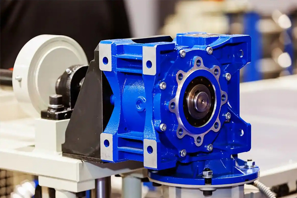
3. Composite Process Capabilities
Surface Treatment Solutions: Chemical Mechanical Polishing (CMP) can achieve a wafer surface roughness of Ra ≤ 0.01nm; Plasma cleaning can remove organic residues on the surface to ensure high cleanliness of components.
Special Coating Processes: Titanium nitride coating (hardness HV2000) can improve the wear resistance of the mold surface; Polytetrafluoroethylene coating (friction coefficient ≤ 0.05) is applied to the moving parts of semiconductor equipment to reduce friction losses.
Key Application Areas
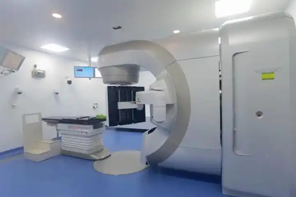
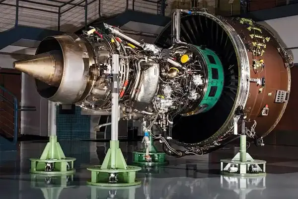
1. Chip Manufacturing Equipment
Components of Lithography Machines: Projection objective lens mounting seats (positioning accuracy ±0.0005mm), reticle clamping devices (flatness ≤ 0.001mm).
Components of Etching Machines: Reaction chambers (high corrosion resistance, surface roughness Ra0.2μm), gas distributors (hole diameter tolerance ±0.001mm).
2. Semiconductor Packaging
Packaging Carriers: Multilayer ceramic carriers (line width/line pitch ≤ 25μm), organic packaging substrates (flatness ≤ 0.02mm).
Lead Frames: Copper alloy lead frames (punching accuracy ±0.01mm) to meet the requirements of high-density packaging.
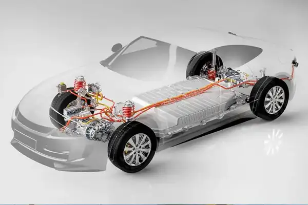
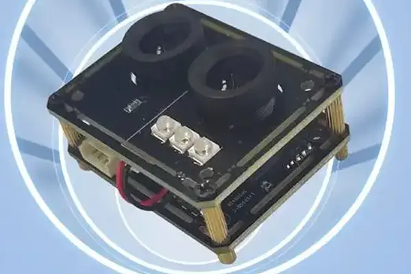
3. Core Components of Electronic Products
Smartphones: Camera module brackets (concentricity ≤ 0.002mm), motherboard heat sinks (heat sink fin pitch ±0.05mm).
Laptop Computers: CPU heat sink bases (flatness ≤ 0.01mm), solid-state drive enclosures (dimensional tolerance ±0.03mm).

Technical Capability Matrix
Indicator |
Parameter |
Highest Machining Accuracy |
Milling ±0.002mm, Lithography Alignment ±0.0005mm |
Typical Surface Roughness |
Ra0.1 - 0.4μm (ultra-smooth surfaces can be customized) |
Batch Production Consistency |
CPK ≥ 1.67 (100% full inspection of critical dimensions) |
Microstructure Machining |
Minimum Line Width/Line Pitch 25μm, Aspect Ratio 10:1 |
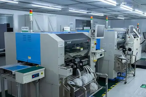
Monthly Standardized Production Capacity |
800,000 precision parts, emergency orders can be responded to within 2 days |
Service Process
1. Requirement Confirmation: Receive drawings/3D models (in CAD/ProE and other formats) and provide DFM manufacturability analysis.
2. Process Development: Develop a process route and complete the PPAP document package (including PSW and MSA reports).
3. Pilot Production Verification: Deliver samples and full-size reports (in line with industry standards).
4. Mass Production Management: Implement SPC process monitoring and support JIT just-in-time supply.
Industry-Recognized Cases
Chip Manufacturing Equipment Project: Mass-produced projection objective lens mounting seats for a well-known domestic semiconductor equipment manufacturer, with an accuracy of ±0.0005mm, and the equipment yield rate increased to 95%.
Semiconductor Packaging Carrier: Processed multilayer ceramic carriers for a leading packaging company, with a line width/line pitch of 25μm, meeting the requirements of advanced packaging processes.
Smartphone Camera Module: Provided camera module brackets for a certain brand of mobile phone, with the concentricity controlled within ±0.002mm, effectively improving the photo clarity.
Additional Value
Compliance Assurance: The material traceability system covers the entire process from raw material procurement to product delivery, supporting the submission of material compliance reports.
Global Collaborative Delivery: Self-operated import and export teams support international logistics customs clearance and quickly respond to the needs of global customers.
Technical Collaborative Development: Jointly optimized the process of 5G base station RF chip heat dissipation structural parts with customers, significantly improving the heat dissipation efficiency.
Get an electronics and semiconductor precision machining solution now →
Submit your technical specifications and receive a complete process plan and tiered quotation within 24 hours!